30m Oscillator (Night 8)
For tonight the theme was trying to get more gain with less current. (This is a theme over the past several nights.)
So I started poking around in Experimental Methods in RF Design... it is pleasure
reading for knack victims. As I started browsing through Chapter 2 intending to read
up on push-pull amps I stumbled across some interesting notes. It was almost a eureka
moment except that I don't understand exactly how to calculate the target RF power
levels yet.
So far I have been largely focused on creating power based upon the DC biased values.
That is important but it does not maximize RF gain and is not as efficient as I might
like it to be. I was getting ~14.6 dBm of gain at a cost of 35mA which is not brilliant.
In the book I noticed a design almost the same as I what I have been working with
but getting almost 20dBm of gain at 20mA.
The difference in the two designs was simple:
1. Don't drive the DC design nearly as hard... I was throwing current at the problem
in brute force fashion.
2. Think about RF.... use some AC coupled feedback to create the gain.

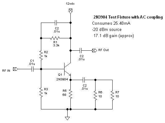
The schematic above is my first attempt to bread board out the idea in the book against
my world and collection of available parts. It looks a LOT like the previous designs
except it is a lower current design with AC coupling between the collector/base and
at the emitter.
Now that I own a nice power meter I ran some tests and captured data.

I measured my signal generator with my power meter, then took down some base values,
and then reran the same test with the 2N3904 amp circuit. I did a little spreadsheet
magic to calculate the gain and then built a graph with the results.
Highlights:
In theory I could probably tweak the resistor values to drive another 2-3dBm of gain
& use a transformer at the RF output to reduce the loading and create a better
match.
In reality I have a good predriver circuit and need to look at some other options
for the next gain stage. (Things like class AB or class C, push-pull amps, or simply
some different parts as I start to transition out of small signal components and into
power.)
Tons of learning tonight. I feel pretty positive about the results. I need to dig
in and better understand the concept of feedback in an amplifier. (35 minutes at the
work bench. 2 hours at the PC working the data and documenting the results.)
73 de NG0R
PS... a quick follow up note after the initial post
I think that the output impedance of this is ~156 ohms.
Ie = Ve / Re or .053 = 3.66/68 (ohms law)
Zout = (Vcc-Vb) / Ie
155.6 = (12.61-4.36)/.053
156 ohms would make sense... you see a lot of these circuits using a 4:1 transformer.
That will transform 200 ohms to 50 ohms which is in the ball park.
PPS... another thought from yesterday's reading & bench time
Rf * Re = Rs * Rl or Rf * Re = Zin & Zout
Rf & Re are the AC coupled components.
(updated below... Re is the total of Re + RE)
In my schematic above I probably should switch the 1K and 3.3K resistors between the
collector and base. That would set Zin to 50 and Zout of 200 approximately.
Something to test. (This is designed for 200 ohms at the moment.)
PPPS.... more math
Rf is the parallel feedback resistor (the AC path)
Re is the net of Re + RE (Re is the DC bias + RE is the AC
degeneration)
Zin & Zout (Input and output impedance.)


So I started poking around in Experimental Methods in RF Design... it is pleasure
reading for knack victims. As I started browsing through Chapter 2 intending to read
up on push-pull amps I stumbled across some interesting notes. It was almost a eureka
moment except that I don't understand exactly how to calculate the target RF power
levels yet.
So far I have been largely focused on creating power based upon the DC biased values.
That is important but it does not maximize RF gain and is not as efficient as I might
like it to be. I was getting ~14.6 dBm of gain at a cost of 35mA which is not brilliant.
In the book I noticed a design almost the same as I what I have been working with
but getting almost 20dBm of gain at 20mA.
The difference in the two designs was simple:
1. Don't drive the DC design nearly as hard... I was throwing current at the problem
in brute force fashion.
2. Think about RF.... use some AC coupled feedback to create the gain.

The schematic above is my first attempt to bread board out the idea in the book against
my world and collection of available parts. It looks a LOT like the previous designs
except it is a lower current design with AC coupling between the collector/base and
at the emitter.
Now that I own a nice power meter I ran some tests and captured data.

I measured my signal generator with my power meter, then took down some base values,
and then reran the same test with the 2N3904 amp circuit. I did a little spreadsheet
magic to calculate the gain and then built a graph with the results.
Highlights:
I can generate about 16-17dBm of gain with about 25mA of power. (That is +3dBm and
-10mA from the previous tests with no AC feedback and strictly DC bias.)
The gain is pretty consistent with -50 to -10dBm of drive source.
The gain falls off very quickly at 0dBm of drive.
As the gain falls off the amp begins to consume a lot of current to produce a small
amount of gain.
The 2N2222 and 2N3904 appear to be good up to about 0dBm of input signal and then
loose their effectiveness. They willl be driving up the harmonic content instead of
the fundamental signal. (I visually saw & measured this on my spectrum analyzer
over the past several nights of testing.)
In theory I could probably tweak the resistor values to drive another 2-3dBm of gain
& use a transformer at the RF output to reduce the loading and create a better
match.
In reality I have a good predriver circuit and need to look at some other options
for the next gain stage. (Things like class AB or class C, push-pull amps, or simply
some different parts as I start to transition out of small signal components and into
power.)
Tons of learning tonight. I feel pretty positive about the results. I need to dig
in and better understand the concept of feedback in an amplifier. (35 minutes at the
work bench. 2 hours at the PC working the data and documenting the results.)
73 de NG0R
PS... a quick follow up note after the initial post
I think that the output impedance of this is ~156 ohms.
Ie = Ve / Re or .053 = 3.66/68 (ohms law)
Zout = (Vcc-Vb) / Ie
155.6 = (12.61-4.36)/.053
156 ohms would make sense... you see a lot of these circuits using a 4:1 transformer.
That will transform 200 ohms to 50 ohms which is in the ball park.
PPS... another thought from yesterday's reading & bench time
Rf * Re = Rs * Rl or Rf * Re = Zin & Zout
Rf & Re are the AC coupled components.
(updated below... Re is the total of Re + RE)
In my schematic above I probably should switch the 1K and 3.3K resistors between the
collector and base. That would set Zin to 50 and Zout of 200 approximately.
Something to test. (This is designed for 200 ohms at the moment.)
PPPS.... more math
Rf is the parallel feedback resistor (the AC path)
Re is the net of Re + RE (Re is the DC bias + RE is the AC
degeneration)
Zin & Zout (Input and output impedance.)

